|
Hardware The Level 64 has been jointly designed by engineers from Honeywell-Bull laboratory in Paris, from Honeywell in Billerica with a small Japanese participation from NEC.
Considering only the products designed by Bull and ignoring momentarily the tentative and aborted projects , three genuine processors have been successively designed:.
In the 1990s, it was decided to discontinue the
design of proprietary processors of DPS-7 product line and to implement
the DP-7000 interior decor to Intel manufactured processors, initially
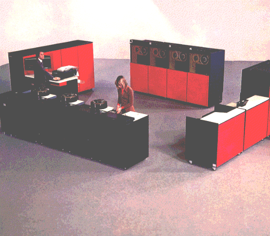
on IA32 Xeon, later on IA64 processors. Those basic processors were implemented in several technologies that allowed (or required) not negligible design changes. In addition, each technical model was delivered in several options leading to different marketing names. Price changes, to match the IBM competition, lead also to new models with sometimes artificial modifications. So, the marketing models identification is somewhat confusing. The initial model was named Level 64. From 1980 to 1987, all models were named DPS-7, and subsequently DPS-7000. The P7 design was based around a 32-bits data bus and a microprogrammed processor. The hardware architecture used a relatively long word and microprograms were fetched from a read-only PROM control store. The same processor circuits was used to interpret the software "decor" instruction set and to handle interrupts from the channel devices. Software visible registers were implemented either in hardware registers or in main memory. A small (but at that time quite expensive) associative memory contained the address translation buffers between the segmented software address and the physical address in main memory. The main memory (max 1 M Bytes) was implemented with 4 Kbits semiconductor chips ( quite new for main frames in the early 70s ). The basic CPU (and peripheral processors) bipolar technology was Texas Instruments 74N small-scale integration chips with a few MSI circuits such as multi-bits multiplexers. P7 was designed in "worst case" design with a guaranteed cycle of 2 MHz and was introduced as two slowed down marketing models the Series 60 64/40 and the 64/50. Tuning the processor on the longer data paths allowed to increase the frequency to 2.5MHz and to introduce a full-speed version of P7, the 64/60.
The P7G project
was launched after the merger between CII and Honeywell-Bull in 1975 and
had the main goal of being substituted to the high-end machine of CII,
the Iris 80 systems (around 50 of them being then in the field). It also
addressed the upgrade of the P7 systems (around one thousand were
delivered in 1979). The new design of P7G was to support up to 4
processors in a true SMP configuration, to handle separately the central
processor and the I/O channel functions and to have a hardware structure
to support the level 64 type of instructions as well as the Iris 80 (itself
derived from the SDS Sigma7). Trouble shooting of the processor by means of an oscilloscope was no more possible with micro packaging and a special mode of CPU operation was to interconnect all chips in a shift register being read and written (to reset the CPU) by the service processor. The clock frequency was set initially at 8 MHz.
In 1982, serious problems were encountered in the reliability of the micro packs. The price of gold (used for chips interconnection in P7G prototype) hiked significantly at that time and, to keep manufacturing costs down, it was decided to change the material of wiring to copper. Copper substrates showed short cuts and breaks due to the electro-migration of copper atoms in the ceramic material and the product line was saved by a come back to gold (the price of gold went down happily). The peak park of the DPS-7 line was reached around 1985 with around 3000 systems, with a majority of them being Taurus systems. The cost of the CML technology remained high and micro packaging was no more applicable to a full range of computer products. After some hesitations (see hereunder) it was decided to reorient the DPS-7 into a CMOS technology.
Ares was modified in 1988 to support paging as well as segmentation (Ares phase 2). A new entry version with a new peripheral architecture was also made available in 1988 (Ares phase 3 or Libra). TCheaper peripherals were coming from the microcomputer world (the most significant being SCSI discs). Instead of reimplementing the peripherals and the channel controllers in a proprietary way, the functions of the original architecture were performed by microprocessor based processor interfacing with the Ares I/O bus. A part from a shift to fixed sectors discs, the new I/O architecture was transparent to software. Ares was not providing a reasonable upgrade path for the Lyra customers and a NEC central system (code named Aquila) was imported from NEC and delivered to customers in 1987. Its interior decor required the implementation of paging and GCOS7 software was modified to support it. Bull Ares and Lyra peripherals, sometimes different from NEC had to be connected to Aquila and checked with the new version (v3B) of GCOS 7. NEC had also to westernize the safety features of its CPU and to adapt to the western specific power supplies. Aquila and Ares allowed a slight increase of the park of customers, but Aqula's cost and its transfer price (including the yen appreciation) did not provide a satisfactory upgrade for Ares customers. So a new CPU design was started targeting an extension to 8 of the number of single board processors, taking advantage of the higher integration available. The Auriga design includes a deeper pipeline, wider data paths, and additional transfer from microprograms interpretation into hardware. A level2 cache was added shared by processors and I/O channels. The Auriga system was introduced as a high end DPS-7000.777
In 1995, it was decide to enhance the DPS-7 product line with the capabilities offered in the Open Systems world. A system code named Diane was implemented. Diane was a system grouping Auriga 2 and Intel Pentium processors used as co-processors. That allowed to unload servers functions running open software in IA32 architecture (running UNIX or Windows 2000) and keeping Mainframe applications under GCOS7. This system allowed a flexible partitioning pioneered in P7G to distribute hardware resources between the cooperating operating systems. A subsequent phase was to take profit of the performance improvements within Intel architecture to develop a DPS-7000 architecture emulator in IA32 and IA64. (Diane 2) In addition, Bull creates several paper designs of processors of this product line. The original design of the product line was the Charlie
project in 1967. It concentrates exclusively on the architecture. In 1973-1974, after the introduction of Level-64, Honeywell-Bull and NEC worked to make an ECL version of P7, called P7-A. Honeywell canceled the project that was continued by NEC on their own. The P7B project was the predecessor of P7G in 1975. Bipolar gate arrays were then considered. When the CII-Honeywell Bull merger became effective in 1977, the project was enhanced to the more powerful P7G using the micro packaging technology designed in GE semiconductor laboratory later transferred to Honeywell. In 1982, Archer, a NMOS project called Archer was started in Les Clayes as a low-end system. Eventually, after the recognition of the CMOS superiority, the project evolved in the successful Ares project. Bull embarks in 1983 (with Digital equipment) backing Gene Amdahl's Trilogy Corp attempt to use the wafer scale integration technology with the intent to use WSI for a high end system called Aquila. After Trilogy's failure, the project was cancelled and the code name was transferred to a non-related NEC-Bull project. In 1987, a first attempt to develop a single chip DPS-7 processor called Altair failed to succeed.
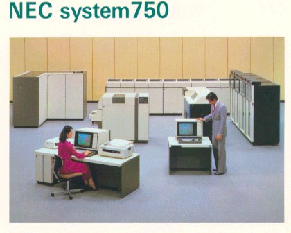
The involvement of NEC in this product line has been already mentioned. NEC was a licensee of Honeywell since the 60s and has produced the H-200 product line Naturally, when Honeywell embarks in Series60, NEC followed and contributed by sending engineers to the project. In 1973, they signed a license agreement for P7, GCOS64 and the architecture with the right to build freely from that basis. The original Honeywell-Bull machine was introduced in Japan as ACOS-450 and the GCOS operating system was delivered as the first release of ACOS4. NEC has made ACOS-4 systems the top of their mainframes competing with the most powerful IBM 3080 and 3090. This strategy was pursued even after the acquisition of the Toshiba business that included the license of GCOS8 36-bits systems that, in Bull and Honeywell, were the most powerful systems. The privileged technology in NEC from 1979
to 1989 was the CML micropackaging, for which NEC developed several
versions of custom-LSI.
It could be noted also that NEC converted its ACOS-2 (alias Level-62, DPS-4) to ACOS-4 by an integrated emulator, while Honeywell and Bull transitioned them by software tools to GCOS-7 and UNIX. NEC enhanced the original architecture first in
introducing 2 and 4 ways multiprocessing, then by introducing the paging.
Those enhancements were based on preliminary designs made with Bull in
1974.
|
||||||||||||
| Index |